| 論文篇名 | 英文:Low-Voltage Operational, Low-Power Consuming and High Sensitive Tactile Switch based on 2D Layered InSe Tribotronics 中文:低電壓、低功耗的二維硒化銦摩擦電晶體與觸覺感測器 |
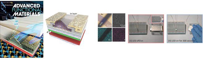
| 期刊名稱 | Advanced Functional Materials (IF=15.621;排名96.96 % (5/148)) ( 獲選Advanced Functional Materials選為封面文章) |
| 發表年份,卷數,起迄頁數 | 2019, 1809119 |
| 作者 | Mengjiao Li,# Feng-Shou Yang,# Yung-Chi Hsiao,# Che-Yi Lin, Hsing-Mei Wu, Shih-Hsien Yang, Hao-Ruei Li, Chen-Hsin Lien, Ching-Hwa Ho, Heng-Jui Liu, Wenwu Li,* Yen-Fu Lin,* and Ying-Chih Lai* |
| DOI | 10.1002/adfm.201809119 |
| 中文摘要 | 此研究利用新穎硒化銦(InSe)二維材料開發低電壓(Vsd=0.1V)、低功耗、高響應(Ion/Ioff>106)的摩擦電電晶體(tribotronic transistor),所實現的元件特性遠優於過去的文獻,我們進一步利用這個成果,實現低電壓操控硒化銦(InSe)二維電晶體的人機介面,有利於未來開發低耗能、低電壓操控的微機電元件,開啟摩擦電子學(tribotronics)與人機介面新的材料研究領域。,此文章刊登於國際頂尖期刊《先進功能材料》(Advanced Functional Materials),被編輯選為封面文章。 |
| 英文摘要 | Electronics based on layered indium selenide (InSe) channels exhibit promising carrier mobility and switching characteristics. Here, an InSe tribotronic transistor (denoted as w/In InSe T‐FET) obtained through the vertical combination of an In‐doped InSe transistor and triboelectric nanogenerator is demonstrated. The w/In InSe T‐FET can be operated by adjusting the distance between two triboelectrification layers, which generates a negative electrostatic potential that serves as a gate voltage to tune the charge carrier transport behavior of the InSe channel. Benefiting from the surface charging doping of the In layer, the w/In InSe T‐FET exhibits high reliability and sensitivity with a large on/off current modulation of 106 under a low drain–source voltage of 0.1 V and external frictional force. To demonstrate its function as a power‐saving tactile sensor, the w/In InSe T‐FET is used to sense “INSE” in Morse code and power on a light‐emitting diode. This work reveals the promise of 2D material–based tribotronics for use in nanosensors with low power consumption as well as in intelligent systems. |
【學術亮點】低電壓、低功耗的二維硒化銦摩擦電晶體與觸覺感測器 2019-05-09
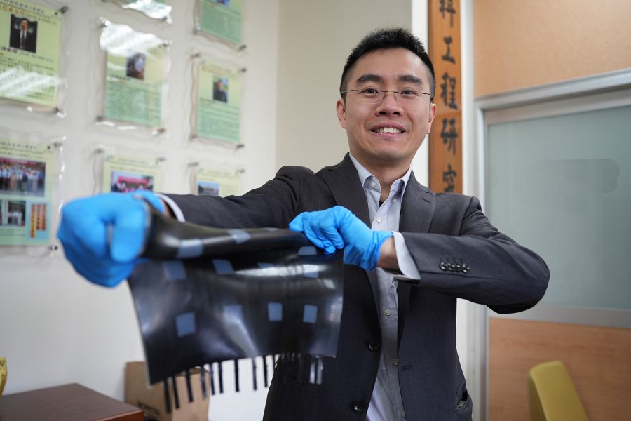
設施農業:綠能設施開發【材料系賴盈至助理教授】