| 論文篇名 | 英文:Tunability of p- and n-channel TiOx thin flm transistors 中文:p型通道與n型通道TiOx薄膜電晶體之可調性 |
| 期刊名稱 | Scientific Reports |
| 發表年份,卷數,起迄頁數 | 2018, 8(1), 9255 |
| 作者 | Wu-Chang Peng, Yao-Ching Chen, Ju-Liang He, Sin-Liang Ou, Ray-Hua Horng, Dong Sing Wuu*(武東星) |
| DOI | 10.1038/s41598-018-27598-5 |
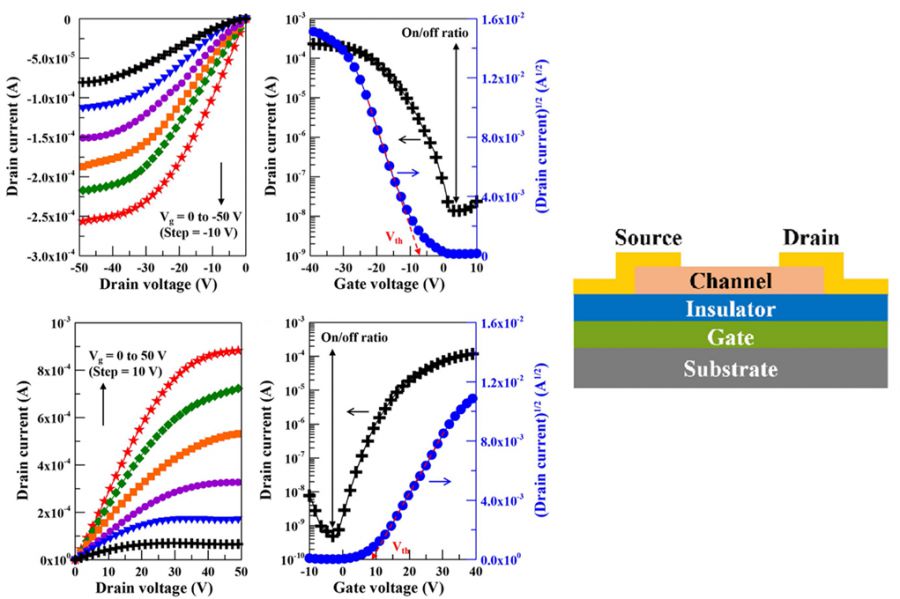
| 中文摘要 | 本研究以高功率脈衝磁控濺鍍(HIPIMS)鍍製氧化鈦薄膜,並製備p型和n型TiOx薄膜電晶體,在鍍膜過程中,透過改變氧氣流量可製備p型γ-TiO和n型TiO2薄膜作為薄膜電晶體的通道層,其p型γ-TiO和n型TiO2薄膜電晶體的場效遷移率(μFE) 分別為0.2與0.7 cm2/Vs,且它們的電流開/關比(Ion/Ioff)分別為1.7×104與2.5×105 。研究結果證實HIPIMS提供了生長p型和n型金屬氧化物半導體的可能性,並且大幅拓展該技術的實際應用性。 |
| 英文摘要 | To acquire device-quality TiOx films usually needs high-temperature growth or additional post-thermal treatment. However, both processes make it very difficult to form the p-type TiOx even under oxygenpoor growth condition. With the aid of high energy generated by high power impulse magnetron sputtering (HIPIMS), a highly stable p-type TiOx film with good quality can be achieved. In this research, by varying the oxygen flow rate, p-type γ-TiO and n-type TiO2 films were both prepared by HIPIMS. Furthermore, p- and n-type thin film transistors employing γ-TiO and TiO2 as channel layers possess the field-effect carrier mobilities of 0.2 and 0.7 cm2/Vs, while their on/off current ratios are 1.7 × 10⁴ and 2.5 × 10⁵, respectively. The first presented p-type γ-TiO TFT is a major breakthrough for fabricating the TiOx-based p-n combinational devices. Additionally, our work also confirms HIPIMS offers the possibility of growing both p- and n-type conductive oxides, significantly expanding the practical usage of this technique. |
【學術亮點】p型通道與n型通道TiOx薄膜電晶體之可調性 2018-06-18
設施農業:節能栽培與滅菌【材料科學與工程學系武東星教授】