設施農業:節能栽培與滅菌【化學工程學系/陳志銘特聘教授】
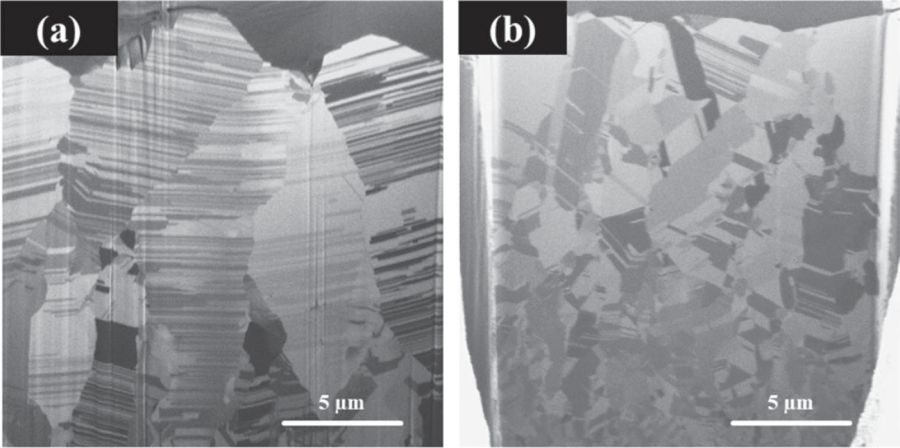
| 論文篇名 | 英文:Electrodeposition of Twinned Cu with Strong Texture Effect on Voiding Propensity in Electroplated Cu Solder Joints 中文:電沉積雙晶銅之高紋理效應對於電鍍銅銲接點孔洞生成傾向之影響 |
| 期刊名稱 | Journal of the Electrochemical Society |
| 發表年份,卷數,起迄頁數 | 2021, 167, no.162516 |
| 作者 | Chiang, Ping-Chen; Shen, Yu-An*; Feng, Shien-Ping; Chen, Chih-Ming(陳志銘)* |
| DOI | 10.1149/1945-7111/abd517 |
| 中文摘要 | 由於在微電子產品中的廣泛應用性,銅的電沉積技術受到許多關注。富錫合金通常使用於連接電鍍銅以形成銲接點,然而它們的相互作用會產生破壞性的柯肯德爾孔洞,而抑制孔洞生成對於確保銲接點機械強度與可靠度至關重要。本研究使用電鍍技術建構具有各種晶體取向的雙晶銅,並研究該結構對孔洞抑制的功效。具有多個雙晶界和不同 (111) 和 (110) 比率的四種銅電鍍層(Cu A、B、C 和 D)與富錫銲料 (SAC305) 結合,並在 200 °C 下進行熱老化。孔洞生成傾向依序為 Cu D > Cu C > Cu B > Cu A,與它們的 (111) 比率成反比(Cu A > Cu B > Cu C > Cu D)。特別地,觀察到由具有大量雙晶竹結結構的電鍍Cu A層,可以建構出無孔洞的銲接點。研究結果亦表明,具有<111>優先取向的竹結結構中的Σ3雙晶邊界,在抑制柯肯德爾效應方面比在<110>優先Cu薄膜中具有更高的效率。 |
| 英文摘要 | Electrodeposition of Cu receives considerable attention due to its wide application in microelectronic products. Sn-rich alloys are commonly used to join the electroplated Cu to form solder joints, while their interactions give rise to undesired Kirkendall voids. Suppression of voids is imperative to ensure reliable solder joints with mechanical robustness. In this study, twinned Cu with various crystal orientations are constructed using electroplating and their efficacy on void suppression are investigated. Four Cu electroplated films (Cu A, B, C, and D) with numerous twin boundaries and different (111) and (110) ratios are joined with Sn-rich solder (SAC305) and thermally aged at 200 °C. The voiding propensity is in an order of Cu D > Cu C > Cu B > Cu A, inversely corresponding to their (111) ratios (Cu A > Cu B > Cu C > Cu D). Particularly, a void-free solder joint constructed by the electroplated Cu A film with plenty of twinned bamboo structures is observed. The findings demonstrate that Σ3 twin boundary in the bamboo structure with 〈111〉-preferred orientation has much higher efficiency at suppressing the Kirkendall effect than that in 〈110〉-preferred Cu films. |
| 發表成果與本中心研究主題相關性 | 透過電沉積技術製作特殊結構的銅金屬層,改善新興元件封裝接點的可靠度。 |

