設施農業:節能栽培與滅菌【材料科學與工程學系/武東星特聘教授】
| 論文篇名 | 英文:Growth characteristics of Fe-doped GaN epilayers on SiC (001) substrates and their effects on high breakdown voltage devices 中文:碳化矽 (001) 基板上之鐵參雜氮化鎵磊晶層的成長機制與高崩潰電壓元件的應用 |
| 期刊名稱 | MATERIALS SCIENCE IN SEMICONDUCTOR PROCESSING |
| 發表年份,卷數,起迄頁數 | 2020, 119, 105228 |
| 作者 | Chang, Kai-Ping; Lin, Po-Jung; Horng, Ray-Hua; Wuu, Dong-Sing(武東星)* |
| DOI | 10.1016/j.mssp.2020.105228 |
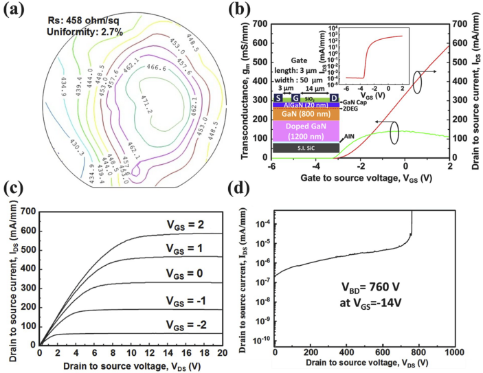
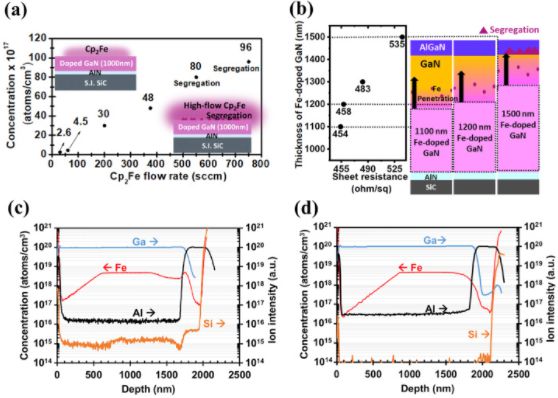
| 中文摘要 | 本研究利用金屬有機化學氣相沉積技術來製作高電子移動率晶體電晶體,並探討此元件於 (001) SiC基板上之Fe摻雜影響,發現通過優化二茂鐵流量可實現光滑的Fe摻雜之GaN外延層表面,而GaN外延層中較高的Fe濃度會影響表面形態,為了減少Fe俘獲載流子和由AlGaN和GaN的界面產生的二維電子氣的薄層電阻,文中優化了摻雜Fe和不摻雜Fe之GaN的雙表層的厚度比,我們已經成功開發了具有Fe摻雜GaN的最佳摻雜濃度和合適厚度的非摻雜GaN AlGaN/GaN高電子移動率晶體電晶體, Fe摻雜的GaN外延層的崩潰電壓可以高達2457V,這歸因於Fe摻雜的GaN外延層具有較高的電阻,可以維持較高的崩潰電壓,本文還將討論用於高擊穿電壓器件的表面形態,Fe濃度和摻雜Fe的GaN外延層厚度之間的相關性。 |
| 英文摘要 | The growth characteristics of Fe-doped GaN epitaxial layers on semi-insulating SiC (001) substrates were studied using metalorganic chemical vapor deposition for high breakdown voltage device applications. A smooth Fe-doped GaN epilayer surface can be realized by changing the ferrocene flow, while higher Fe concentrations in the GaN epilayer affect the surface morphology. To reduce the Fe trapping carrier and the sheet resistances of the two-dimension electron gas generated from the interface of AlGaN and GaN, the thickness ratio of Fe-doped and undoped GaN bi-epilayers was also optimized. AlGaN/GaN high electron mobility transistors with the optimum doping concentration of Fe-doped GaN and suitable thickness of undoped GaN have been successfully developed. The achieved breakdown voltage of the Fe-doped GaN epitaxial layer can be as high as 2457 V, which is attributed to the Fe-doped GaN epitaxial layer with higher resistance, which can sustain the high breakdown voltage. The details of the correlation between the surface morphology, Fe concentration, and thickness of Fe-doped GaN epitaxial layers used for high breakdown voltage devices will be also discussed in this paper. |
