設施農業:節能栽培與滅菌【化學工程學系/陳志銘特聘教授】
| 論文篇名 | 英文:Effects of Impurities on Void Formation at the Interface between Sn-3.0Ag-0.5Cu and Cu Electroplated Films 中文:雜質摻雜對錫銀銅與電鍍銅接合界面孔洞生成的影響 |
| 期刊名稱 | Journal of Materials Science: Materials in Electronics |
| 發表年份,卷數,起迄頁數 | 2021, 32, 11944–11951 |
| 作者 | Chiang, Ping-Chen; Shen, Yu-An*; Chen, Chih-Ming(陳志銘)* |
| DOI | 10.1007/s10854-021-05824-7 |
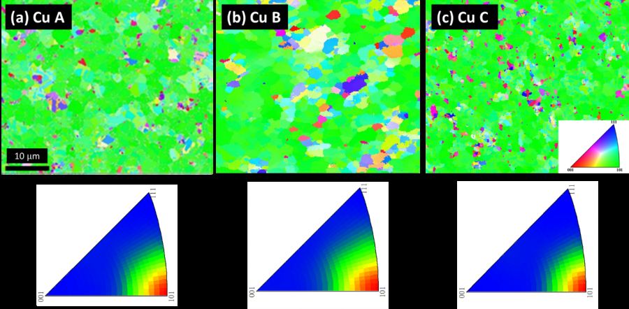
| 中文摘要 | 孔洞生成是電子封裝銲接點的關鍵可靠度問題,微觀結構的控制和銅電鍍膜中雜質的數量顯著影響接點界面的孔洞生成,但相關研究甚少。在本研究中,使用電鍍工藝製造三種銅膜( A、B 和 C)。A銅 膜具有嵌入雙晶界的刻面晶粒紋理,而B銅膜和C銅膜具有相似的柱狀紋理。在 200 °C 下熱老化 1000 小時後,帶有A銅膜和B銅膜的 SAC 305 (Sn-3.0Ag-0.5Cu) 銲接點表現出堅固的界面結構,同時沒有孔洞生成。然而,在 SAC 305/C銅膜的銲點中觀察到顯微結構塌陷,其中許多裂縫平行於界面生成。根據微量分析,C銅膜中的雜質濃度高於A 和 B銅膜。此外,當降低C銅膜中的雜質濃度時,SAC305/C銅膜系統中會出現離散的空隙而不是連續的裂縫。研究結果表明,銅電鍍膜中的雜質控制對於控制電子銲點中的孔洞/裂縫形成至關重要。 |
| 英文摘要 | Void formation is a critical reliability concern for solder joints in electronic packaging. The control of microstructures and the quantity of impurities in Cu electroplated films significantly affect void formation at the joint interface, but studies investigating these factors are rare. In this study, three Cu films (denoted as A, B, and C) are fabricated using an electroplating process. The Cu A film has a faceted grain texture embedded with twin boundaries, while Cu B and C films have similar columnar textures. After thermal aging at 200 °C for 1000 h, the SAC 305 (Sn-3.0Ag-0.5Cu) solder joints with Cu A and B films exhibit robust interfacial structures without voids. However, microstructural collapse is observed in the solder joint of SAC 305/Cu C, where many crevices are formed parallel to the interface. Based on the microanalysis, the concentration of impurities is higher in Cu C than in Cu A and B. Moreover, discrete voids rather than continuous crevices are present in the SAC305/Cu C system when the impurity concentration in Cu C is reduced. The findings demonstrate that impurity control in Cu electroplated film is critical for the control of void/crevice formation in electronic solder joints. |
| 發表成果與本中心研究主題相關性 | 透過電沉積技術製作特殊結構的銅金屬層,改善新興元件封裝接點的可靠度。 |

