設施農業:綠能設施開發【材料科學與工程學系賴盈至教授/優聘教師】
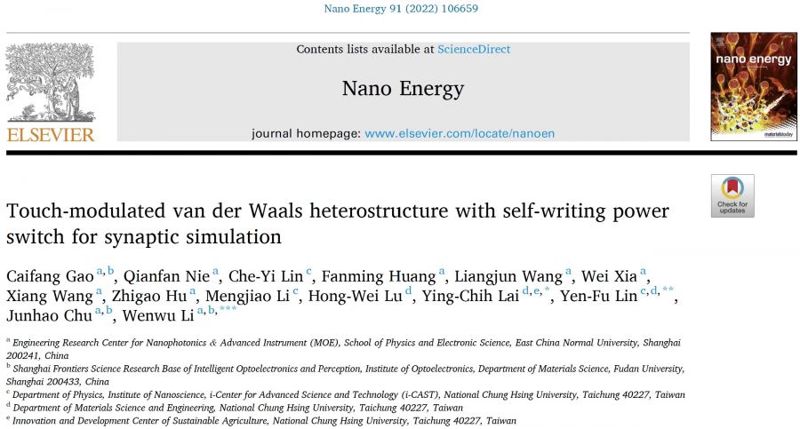
| 論文篇名 | 英文:Touch-modulated van der Waals heterostructure with self-writing power switch for synaptic simulation 中文:受 Mycena Chlorophos 啟發的自發光摩擦電纖維,用於可穿戴能量收集、自供電傳感和人機界面 |
| 期刊名稱 | NANO ENERGY |
| 發表年份,卷數,起迄頁數 | 2022, 91, 106659. |
| 作者 | Gao, Caifang; Nie, Qianfan; Lin, Che-Yi; Huang, Fanming; Wang, Liangjun; Xia, Wei; Wang, Xiang; Hu, Zhigao; Li, Mengjiao; Lu, Hong-Wei; Lai, Ying-Chih(賴盈至)*; Lin, Yen-Fu; Chu, Junhao; Li, Wenwu |
| DOI | 10.1016/j.nanoen.2021.106659 |
| 中文摘要 | 摩擦電子學(tribotronics)是接觸起電奈米發電機的一個研究領域,主要研究材料表面電荷與外在環境因子(如觸摸、壓力、加速度、震動等)耦合對半導體元件的電性變化,可應用於新型微機電元件。 其中,將接觸起電奈米發電機導入電晶體元件,可將三點(閘極-源極-汲極)元件簡化成兩點(源極-汲極)元件,並利用外面環境因子調控閘極偏壓,達成感測環境因子的功能。另一方面,利用二維材料製作的類神經電子元件,具有小型化、低功耗的優勢,對於低功耗電子設備的發展具有相當潛力。 此研究中,我們提出一種基於硒化銦(InSe)/六方氮化硼(h-BN)/石墨烯(graphene)的類突觸電晶體,並且與接觸起電奈米發電機耦合,成功實現自發電觸覺學習的類突觸電晶體。此類突觸電晶體具有829 cm2 V-1 s-1 的高遷移率、0.02 V的低電壓、多位數據存儲、零寫入功率的特性。無需額外的閘極電源,可直接利用觸摸學習,執行記憶電晶體的寫入功能,在165 aJ 的超低功耗下,成功模仿觸覺記憶突觸的可行性。此自發電二維材料類突觸電晶體的實現,可作為二維材料元件在低功耗神經形態電子系統、人工智能與微機電元件的典範。 |
| 英文摘要 | Neuromorphic electronics with two-dimensional van der Waals materials meet the ever-increasing demands of both the semiconductor industry and biological engineering, such as miniaturization, structure flexibility, multifunctionality, and low power consumption. However, the majority of reported electronic devices achieve multifarious memory storage states or synaptic plasticity through regulation of an electrical or an optical signal. Herein, we propose an innovative touch-modulated device based on an indium selenide/hexagonal boron nitride/graphene van der Waals heterostructure coupled with a triboelectric nanogenerator. The device is prepared utilizing a simple copper grid shadow mask instead of the expensive and cumbersome electron beam lithography process, exhibits high mobility of 829 cm2 V−1 s−1, low voltage, and low power consumption. Nonvolatile memory with self-writing power, durability and multibit data storage is achieved through mechanical modulation without an additional gate-voltage supply. Moreover, by adjusting the distance between the two friction layers, essential synaptic plasticity, including short-term and long-term potentiation/depression and paired-pulse facilitation/depression, are successfully imitated in the device. Most importantly, we achieve ultralow power consumption of 165 aJ in tribotronic synapses owing to the ultra-high mobility of InSe. Our tribotronic synapse with self-writing power has great potential to simulate the low-power-consuming neuromorphic bioelectronic devices with multiple functions and lays the foundation for future advanced neuromorphic systems and artificial intelligence. |
| 發表成果與本中心研究主題相關性 | 實現低功耗運算電晶體,未來可用於農業感測物聯網。 |

