設施農業:節能栽培與滅菌【材料科學與工程學系/武東星特聘教授】
| 論文篇名 | 英文:Improvement of p-electrode structures for 280 nm AlGaN LED applications 中文: 280 奈米波長之氮化鋁鎵發光二極體的P型電極結構優化與應用 |
| 期刊名稱 | SEMICONDUCTOR SCIENCE AND TECHNOLOGY |
| 發表年份,卷數,起迄頁數 | 2020, 35, 105023 |
| 作者 | Chang, Kai-Ping; Jheng, Jhih-Yuan; Huang, Shih-Yung; Wang, Wei-Kai; Horng, Ray-Hua*; Wuu, Dong-Sing(武東星)* |
| DOI | 10.1088/1361-6641/abaaee |
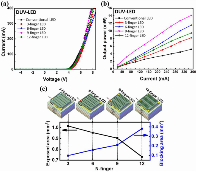
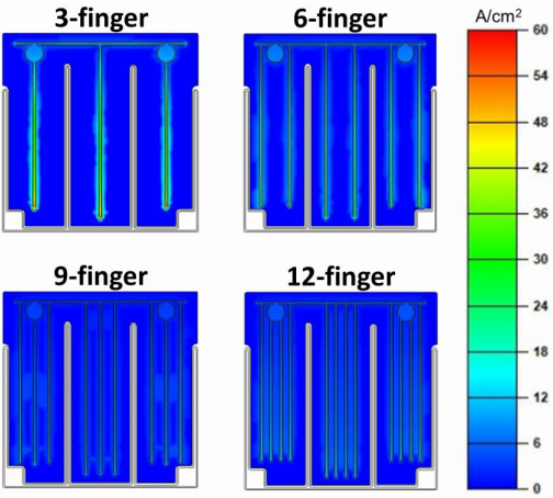
| 中文摘要 | 本文提出了針對280 奈米發光波長的AlGaN深紫外發光二極體之Ni/Au/p -GaN P型電極和倒晶封裝結構優化。在p型電極側朝上的深紫外發光LED中採用了叉指式多指Ni / Au,其中部分去除了p-GaN接觸層以提高光提取效率,而沒有嚴重的電流擁擠效應。其中9指和12指電極之LED具有更高的散熱和更低的表面溫度,並且與模擬數據具有高度的相關性。為了比較p側朝上發射的LED,在注入電流為350 mA時,9指LED的輸出功率比傳統LED高172%,此最佳的p電極布局可進一步應用於倒裝芯片LED結構。可以確定的是,九指倒晶封裝之LED在350 mA時的輸出功率仍比常規倒裝芯片LED高14.6%。9指倒裝芯片LED也具有1.05%插座效率,更高輸出功率歸因於改進的電流分佈路徑和最佳化之p -GaN吸收層與反射層面積。 |
| 英文摘要 | An improvement of Ni/Au/p -GaN p-electrode for AlGaN deep-ultraviolet light-emitting diodes (DUV LEDs) with the emission wavelength of 280 nm is proposed for both p-side-up and flip-chip structures. An interdigitated multi-finger Ni/Au was employed in p-side-up DUV LED, where the p-GaN contact layer was partially removed to improve the light extraction efficiency without a serious current-crowding effect. The 9- and 12-finger LEDs were determined to have higher thermal dissipation and lower surface temperatures and correlated well with the theoretical simulation. For the comparison of p-side-up emission LEDs, the output power of 9-finger LED is 172% higher than that of conventional LED at the current injection of 350 mA. The optimum p-electrode pattern was further applied to the flip-chip LED structure. It is determined that the output power of 9-finger flip-chip LED at 350 mA is still 14.6% higher than that of a conventional flip-chip LED. The higher output power of 9-finger flip-chip LED with a wall-plug efficiency of 1.05% is attributed to the combination of the improved current-spreading path and the higher reflection through the moderate removal of partial p -GaN absorbing layer. |
