【學術亮點】Microstructures of Sn-5Sb/Sn-58Bi mixed solder and its interfacial reaction with copper
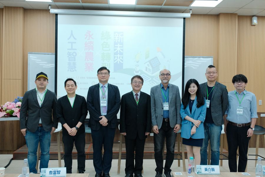
Facility Agricultural: Green Energy Development and Carbon Offset【Department of Chemical Engineering / Chen, Chih-Ming/ Distinguished Professor】
設施農業:農業綠能開發與碳匯補償【化學工程學系陳志銘 特聘教授】
| 論文篇名 | 英文:Microstructures of Sn-5Sb/Sn-58Bi mixed solder and its interfacial reaction with copper 中文:錫-5銻/錫-58鉍混合銲料的微觀組織及其與銅的界面反應 |
| 期刊名稱 | Journal of Materials Science: Materials in Electronics |
| 發表年份,卷數,起迄頁數 | 2025, 36, no.469 |
| 作者 | Li, Yue; Li, Yu-Ju; Chung, Man-Hsuan; Chen, Chih-Ming(陳志銘)* |
| DOI | 10.1007/s10854-025-14541-4 |
| 中文摘要 | 熱致動態翹曲是大尺寸、多層封裝結構的關鍵可靠度問題。採用低溫銲料降低焊接溫度是減少封裝翹曲影響的潛在解決方案。低溫銲料製程透過使用網版印刷在電路板上的低溫銲膏來鍵合封裝側面的球柵陣列銲球來實現。在本研究中,使用共晶錫-58鉍銲料(15.8 mg) 與錫-5銻銲球 (22 mg) 在 160 °C、180 °C 和 200 °C 下鍵合 3 分鐘,之後使用顯微鏡觀察和相圖研究混合銲料的微觀結構演變。連接到銅基板的混合銲料在 125 °C 下加熱長達 480 小時,以觀察接點界面處玠金屬化合物的生長。在200 ℃焊接溫度下,觀察到成分為錫-24.3 wt.% 鉍-2.9 wt.% 銻的完全混合銲料,凝固合金中形成了粗大(鉍)相彌散分佈於連續(錫)基體中的兩相組織,銻溶解於兩相中。在銲料/銅界面處形成Cu6Sn5相和Cu3Sn相,而Cu3Sn相的生長速度與Cu6Sn5相相比非常緩慢。在125 ℃固態時效提高鉍在錫中的溶解度,減少了粗大(鉍)顆粒的數量,同時在凝固合金中產生了許多細小的(鉍)析出物。 |
| 英文摘要 | Thermally induced dynamic warpage is a critical reliability issue for large-size and multi-level package structures. Reduction of soldering temperature with low temperature solder (LTS) is a potential solution to reduce the impacts of package warpage. The LTS process is implemented by using a low temperature solder paste screen-printed on the board to bond the ball-grid-array (BGA) solder balls attached on the package side. In this study, eutectic SnBi solder (15.8 mg) was used to bond with Sn-5 wt.% Sb solder ball (22 mg) at 160 °C, 180 °C, and 200 °C for 3 min, after which the microstructural evolution of mixed solder was investigated using microscopic observation and phase diagrams. The mixed solder joined to the Cu substrate was heated at 125 °C for up to 480 h to observe the growth of intermetallic compounds at the joint interface. Fully mixed solder with a composition of Sn-24.3 wt.% Bi-2.9 wt.% Sb was observed at the soldering temperature of 200 °C, producing a two-phase microstructure of bulky (Bi) phase dispersed in the continuous (Sn) matrix in the solidified alloy, with Sb dissolving in the two phases. The Cu6Sn5 and Cu3Sn phases were formed at the solder/Cu interface, while the Cu3Sn phase exhibited a very sluggish growth rate compared to that of Cu6Sn5. Solid-state aging at 125 °C increased the solubility of Bi in Sn, reducing the quantity of bulky (Bi) particles while producing many fine (Bi) precipitates in the solidified alloy. |
| 發表成果與本中心研究主題相關性 | 封裝銲點存在於各式能源元件與設備之中,了解銲點性能有助於改善元件的運作效能與信賴性。 |