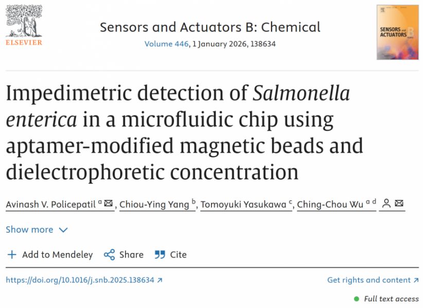
【學術亮點】Nanograin-Twin-Nanograin Alternating Composite Structure Enable Improved Cross-Interface Cu-Cu Bonding at Low Thermal Budgets
Facility Agricultural: Green Energy Development and Carbon Offset【Department of Chemical Engineering / Chen, Chih-Ming/ Distinguished Professor】
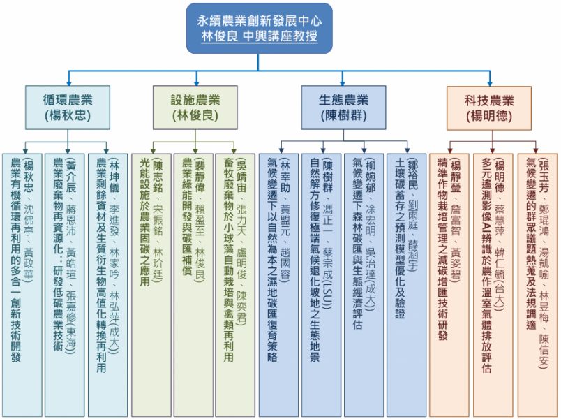
設施農業:農業綠能開發與碳匯補償【化學工程學系陳志銘 特聘教授】
| 論文篇名 | 英文:Nanograin-Twin-Nanograin Alternating Composite Structure Enable Improved Cross-Interface Cu-Cu Bonding at Low Thermal Budgets 中文:奈米晶-奈米雙晶-奈米晶交替複合結構可在低熱預算下改善跨界面銅-銅鍵合 |
| 期刊名稱 | Small Methods |
| 發表年份,卷數,起迄頁數 | 2025, 9(9), e00831 |
| 作者 | Chen, Cong; Li, Helios Y.; Peng, Gangqiang; Zheng, Zeyang; Dong, Erqian; Zhong, Jianwen; He, Chuan; Wang, Yi; Chang, Jia-Syuan; Gan, Zhuofei; Gao, Jinwei; Huang, Yu-Ting; Chen, Chih-Ming(陳志銘)*; Feng, Shien-Ping |
| DOI | 10.1002/smtd.202500831 |
| 中文摘要 | 採用矽通孔和直接銅-銅鍵結技術的晶片堆疊已成為克服摩爾定律限制的卓越解決方案。然而,傳統方法面臨一個根本性的權衡:粗晶粒銅需要較高的鍵合溫度 (>300 °C),而奈米晶粒銅不穩定,即使在室溫下電鍍後也容易粗化。本研究提供一種獨特的複合銅架構,該架構具有交替的奈米晶粒和(111)取向奈米雙晶。由共格雙晶界穩定的奈米雙晶銅抑制室溫晶粒的生長(15 天內電阻漂移 2%),而奈米晶銅區域則使晶粒在 170 °C 下快速生長。這種雙重功能透過兩種協同途徑促進界面原子橋接:1)以晶界擴散為主的奈米晶銅再結晶;2)沿著奈米雙晶銅(111)面的低活化能表面遷移。由此產生的鍵結實現增強的機械和電氣性能:56.4±3.6 MPa的剪切強度(52% > 粗Cu),258小時的電遷移壽命(6.45倍 > 常規Cu),以及1000次熱循環(-16至160 ℃)後的電阻漂移為3.1%。這項工作不僅為低熱預算的三維封裝提供實用的解決方案,也為設計能夠調和傳統不相容特性的亞穩態複合材料建立範例。 |
| 英文摘要 | Chip stacking using through-silicon via (TSV) and direct copper-to-copper (Cu─Cu) bonding technology has emerged as a superior solution to overcome the limitations of Moore's law. However, conventional approaches face a fundamental trade-off: coarse-grained Cu requires high bonding temperatures (>300 °C), while nanograined Cu is unstable and tends to coarsen even at room temperature after electroplating. Here, this paradigm is broken through a unique composite copper (comp-Cu) architecture featuring alternating nanograin (ng─Cu) and (111)-oriented nanotwin (nt─Cu) domains. The nt─Cu domains, stabilized by coherent twin boundaries (CTBs), suppress room-temperature grain growth (2% resistance drifts over 15 days), while ng─Cu regions enable rapidly grain growth at 170 °C. This dual functionality facilitates atomic bridging across interfaces via two synergistic pathways: 1) grain-boundary-diffusion-dominated ng─Cu recrystallization and 2) low-activation-energy surface migration along nt─Cu (111) planes. The resulting bonded joints achieve enhanced mechanical and electrical performance: 56.4±3.6 MPa shear strength (52% > coarse Cu), 258 h electromigration lifetime (6.45× > conventional), and 3.1% resistance drift after 1,000 thermal cycles (−16–160 °C). The work not only provides a practical solution for low-thermal-budget 3D packaging but also establishes a paradigm for designing metastable composites that reconcile traditionally incompatible properties. |
| 發表成果與本中心研究主題相關性 | 封裝銲點存在於各式能源元件與設備之中,發展高性能接合技術有助於改善元件的運作效能與信賴性。 |