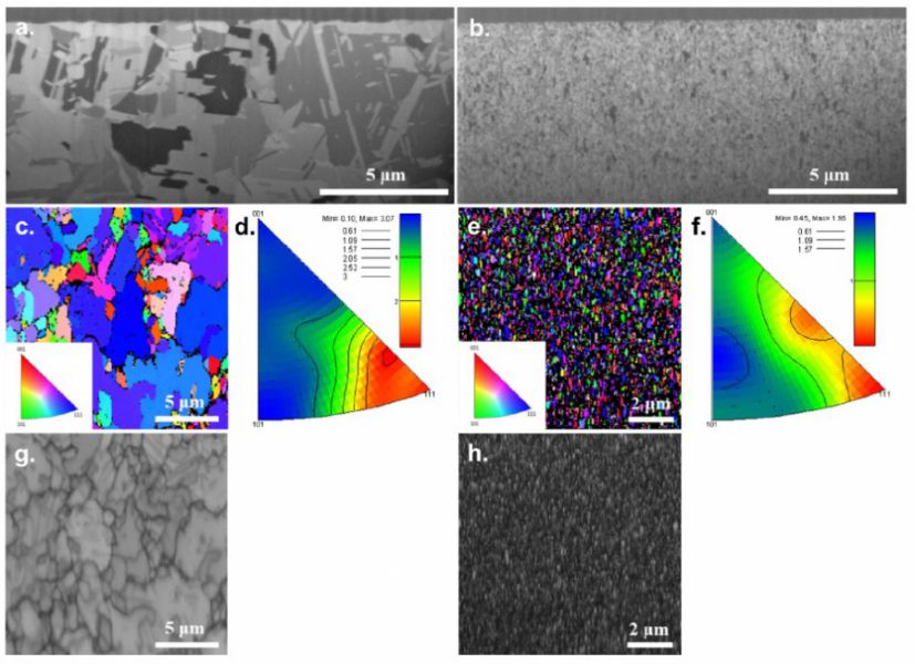
| 論文篇名 | 英文:Study of grain size effect of Cu metallization on interfacial microstructures of solder joints 中文:銅金屬層晶粒尺寸效應對銲點界面微觀結構影響之研究 |
| 期刊名稱 | Microelectronics Reliability |
| 發表年份,卷數,起迄頁數 | 2019, Vol. 99, pp. 44-51 |
| 作者 | Zeyang Zheng, Ping-Chen Chiang, Yu-Ting Huang, Wei-Ting Wang, Po-Chien Li, Ya-Hui Tsai, Chih-Ming Chen, and Shien-Ping Feng |
| DOI | 10.1016/j.microrel.2019.05.018 |
| 中文摘要 | 採用直流電沉積法製備了不同粒徑與不同硬度的銅薄膜,包括細銅(~1.3 μm,~0.85 Gpa)與奈米銅(~100 nm,~1.94 Gpa)。使用聚焦離子束和電子背散射繞射研究薄膜的微觀結構。採用X射線繞射和奈米壓痕儀研究銅薄膜的結構和硬度。研究結果顯示,隨著電流密度的增加,電鍍銅層(200)紋理與硬度均提高。為研究這兩種銅膜銲點的界面反應,製備Sn-3 wt%Ag-0.5 wt%Cu/Cu和Sn-3.5 wt%Ag/Cu兩種銲點,在150 °C下對其進行熱退火處理,結果顯示,細銅具有良好的緻密界面,而奈米銅則在銲點界面處生成孔洞,二次離子質譜分析結果顯示孔洞生成與奈米銅中具有較高雜質含量有關。因此,銲點界面形貌與銅晶粒尺寸之間的相關性顯示,晶界在控制銅膜硬度和雜質以及銲點可靠性方面有顯著的作用。 |
| 英文摘要 | Cu films owing different grain size and hardness in terms of fine copper (~1.3 μm, ~0.85 GPa) and nano copper (100 nm, ~1.94 GPa) were fabricated through direct current (DC) electroplating. The film microstructures were investigated using focused ion beam (FIB) and electron backscattered diffraction (EBSD). Texture and hardness of the Cu films were studied by X-ray diffraction (XRD) and nanoindentation. The results indicated a growing (200) texture and higher hardness along with the increase of current density. To study the interfacial reactions of the solder joints based on the two Cu films, the Sn-3 wt% Ag-0.5 wt% Cu/Cu and Sn-3.5 wt% Ag/Cu joints were prepared and thermally aged at 150 °C. The fine-Cu exhibited an excellent compact interface, while nano-Cu suffered from void formation at the joint interface. The secondary ion mass spectrometer (SIMS) analysis correlated the results with higher impurity level in nano-Cu. Thus, the strong dependence between interfacial morphology of solder joints and Cu grain size indicated an important role of grain boundary in controlling the hardness and impurities of Cu films along with its reliability of the solder joints. |
【學術亮點】銅金屬層晶粒尺寸效應對銲點界面微觀結構影響之研究 2019-05-27
設施農業:節能栽培與滅菌【化工系陳志銘特聘教授】


